
Full ASIC back-end physical design of an OV7670-based camera controller — RTL-to-GDS using Synopsys DC + ICC2 on the SAED32nm RVT process node.
Forked from amsacks/OV7670-camera (FPGA-original), then reworked for ASIC compatibility and taken through a complete physical design flow.
The OV7670 captures real-time video at 640×480 @ 30 fps over an 8-bit parallel interface and outputs it over VGA. This project adapts that RTL for ASIC tape-out (educational), resolving FPGA-specific constructs (tri-state SDA, BRAM inference), fixing multi-clock domain issues across three asynchronous clocks (i_top_clk, w_clk25m, i_top_pclk), and running the design through synthesis, place & route, and signoff using Synopsys industrial tools.
| Parameter | Value |
|---|---|
| Technology | SAED 32nm RVT (1P9M) |
| Supply Voltage | 0.95 V (nom) |
Target Clock (i_top_clk) |
100 MHz (10 ns period) |
VGA Pixel Clock (w_clk25m) |
25 MHz (40 ns period) |
Camera Clock (i_top_pclk) |
Asynchronous input |
| Core Area | 4261.99 µm² |
| Chip Area | 7273.36 µm² |
| Leaf Cells (netlist) | 273 |
| Total Leaf Cells (with filler) | 1771 |
| Flip-Flops | 57 |
| ICG Cells | 6 |
| Total Wire Length | ~4096 µm |
The top-level design (top) integrates the following sub-blocks:
OV7670_cam— Camera controller with SCCB (I²C-like) configuration engineconfigure_cam— register sequencer driving the OV7670 over SCCBSCCB_HERE— bit-bang serial controller (SDA, SCL)
display_interface— VGA timing signal generator (640×480, 60 Hz)vga_timing_signals— horizontal/vertical counter logic (clocked byw_clk25m)
BRAM-based frame buffers from the original FPGA design were replaced — the register array (reg [WIDTH-1:0] ram [0:DEPTH-1] at 640×480 depth) would have inferred ~3.37M flip-flops and is fundamentally incompatible with standard-cell ASIC synthesis.
RTL (Verilog)
    │
    ▼
Synopsys Design Compiler (dc_shell W-2024.09)
    │  SAED32RVT SS corner  |  3 async clocks  |  clock gating
    ▼
Synopsys IC Compiler II (icc2_shell W-2024.09)
    │  Floorplan → Power Planning → Placement → CTS → Route → Signoff
    ▼
GDS (gdsout/)
Scripts:
| Script | Purpose |
|---|---|
run_dc.tcl |
Synthesis with SAED32RVT, multi-corner constraints |
run_icc2.tcl |
Full PnR flow — floorplan through route + signoff checks |
run_pt.tcl |
PrimeTime STA (post-route) |
run_all.sh |
Sequential wrapper for full flow |
Library: saed32_rvt NDM — SS/FF corners, –40°C to 125°C, 0.75V–1.16V
| Clock Domain | Period | Critical Path | Slack | TNS | Violations |
|---|---|---|---|---|---|
i_top_clk |
10 ns | 0.88 ns | +8.90 ns | 0 | 0 |
w_clk25m |
40 ns | 0.96 ns | +38.83 ns | 0 | 0 |
| reg2out | 10 ns | 0.66 ns | +5.24 ns | 0 | 0 |
| in2out | 10 ns | 0.15 ns | +5.75 ns | 0 | 0 |
Setup (max delay): Critical path — SCCB_HERE/r_data_bit_index_reg[7] → o_top_sda_oe, 4 logic levels, slack +5.24 ns (MET)
Hold (min delay): Critical path — vga_timing_signals/hc_reg[0], slack +0.14 ns (MET)
All timing paths met across both func_fast and func_slow scenarios. Zero TNS, zero hold violations.
| Check | Result |
|---|---|
| Short violations | 0 |
| Open nets | 0 |
| Floating routes (VDD/VSS power rings) | 2 (informational — no signal shorts) |
LVS: CLEAN — no connectivity errors on 317 signal/clock/power nets.
| Rail | Std Cells Connected | Disjoint Sub-networks |
|---|---|---|
| VDD | 1771 | 1 (isolated 4-wire stub — power ring artifact) |
| VSS | 1771 | 1 (isolated 4-wire stub — power ring artifact) |
No floating standard cells, no unconnected ports.
| Violation Type | Count |
|---|---|
| Diff-net variable rule spacing | 3 |
| Same-net via-cut spacing | 26 |
| Total | 29 |
Remaining DRCs are spacing rule violations from power stripe / signal congestion interaction on M1. Antenna checking was not active for this run.
| Category | Area (µm²) | % |
|---|---|---|
| Combinational logic | 414.76 | 48.5% |
| Sequential (FF + ICG) | 440.69 | 51.5% |
| Buffer/Inverter | 75.48 | — |
| Filler cells | 3406.55 | — |
| Total cell area | 855.45 | — |
| Core area | 4261.99 | — |
| Chip area | 7273.36 | — |
| Layer | Signal Wires | Wire Length |
|---|---|---|
| M1 | 252 (13.2%) | 69.4 µm |
| M2 | 1012 (53.1%) | 1140.8 µm |
| M3 | 538 (28.2%) | 1141.8 µm |
| M4 | 86 (4.5%) | 525.3 µm |
| M5 | 19 (1.0%) | 109.4 µm |
Total vias: 6262 | Double-via conversion rate: 59.1% (97.4% on detail-route vias)
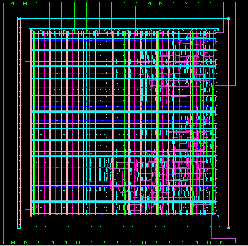
OV7670-camera-asic/
├── rtl/                # Verilog RTL (ASIC-adapted)
├── tb/                 # Testbenches
├── synthesis/          # DC outputs (netlist, reports)
├── floorplanning/      # ICC2 floorplan snapshots
├── placement/          # Post-placement views
├── signoff/            # LVS, timing, DRC reports
├── strategies/         # ICC2 strategy files
├── gdsout/             # Final GDS
├── run_dc.tcl          # Synthesis script
├── run_icc2.tcl        # PnR script
├── run_pt.tcl          # STA script
└── run_all.sh          # Full-flow runner
Frame Buffer (BRAM → SRAM)
The original FPGA design uses mem_bram.v — a 640×480 register array that cannot be synthesized for ASIC. A dedicated SRAM macro is required. Options:
- OpenRAM for an open-source SRAM compiler
- Synopsys/Cadence proprietary memory compilers (licensed)
Until this is resolved, the frame buffer is excluded from the netlist. The camera capture + VGA timing logic synthesizes and routes cleanly.
Remaining DRCs (29) Post-route DRC violations are spacing issues on M1 between power stripes and signal routes in congested regions. Root cause: power mesh on M1 conflicting with signal routing during detail route. Resolution would require either spreading the floorplan or adjusting power stripe pitch.
Tri-state SDA
The original inout sda was refactored to separate i_sda_in / o_sda_oe ports for ASIC compatibility (tri-states not supported in standard-cell flows).
- Synopsys Design Compiler
W-2024.09— RTL synthesis - Synopsys IC Compiler II
W-2024.09— Place & Route, signoff DRC/LVS - Synopsys PrimeTime
T-2022.03-SP2— Static timing analysis - Library: SAED32nm RVT standard cells (1P9M, educational PDK)
Original RTL design by @amsacks — FPGA implementation targeting Xilinx Basys 3.
ASIC adaptation, synthesis, PnR, and signoff by @xp4t.